|
Audio Time Delay Systems
AN AUDIO BUFF is constantly seeking ways to make the sound from his audio system more realistic. That’s why there’s been a high level of interest in a family of audio components known as audio delay lines or “room expanders.” Such a component is intended to create an auditory illusion that simulates the environment in which music is ordinarily performed—a large concert hall, a night club, etc.—rather than the sense of being reproduced in a small listening room.
IN THIS three-part series, we present two different types of audio delay lines, either of which can be built by a technically inclined audiophile for a relatively moderate cost. The delay line described this month and next is an analog design. Part three’s project employs digital signal-storage techniques.
A Low-Cost Analog Audio Delay line
Analog system employs a bucket-brigade device and compansion to provide adjustable delays and wide dynamic range
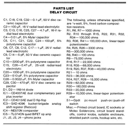
THE analog audio delay line described here employs a high-performance, “bucket-brigade” analog shift register and a 2:1 compansion system to preserve as much of the input signal’s dynamic range as possible. According to its designer, it offers an adjustable delay time of from 5 to 68 ms, a frequency response of 30 to 12,000 Hz (+0, —1 dB), an output noise rating (“A” weighted) of —91.5 dBm at 5ms delay, and a TI-ID + N content of 1% at 10 kHz. A complete stereo delay-line kit including an ac or dc power supply and a custom enclosure is available for $250.
Delay Lines and Reverberation. Perhaps the most significant difference between a large concert hall and the typical home listening room lies in their reverberation times. Reverberation time can be de fined as the amount of time it takes for a steady-state sound field to decay to —60 dB relative to the level that existed before the sound source was deactivated. The size of a room and the materials used to construct it affect its reverberation time.
Because the speed of sound in air is relatively constant (approximately one foot or 0.3 meter per millisecond) for given atmospheric conditions, sound waves traveling in a very large room will experience fewer energy-absorbing collisions with the walls, floors, and ceiling per unit time than will similar sound waves traveling in a small room. Accordingly, sound waves in the large room decay less rapidly.
A listener in a reflective room receives a series of sound waves starting with the wave that reaches him on a direct path from the source. The reflected waves arrive at some time after the direct signal. The human ear derives from these differences in arrival times clues as to the size of the listening space.
When the reflections arrive so soon after the direct wave that they merge with it, the room “sounds” small. By contrast, larger differences in arrival times and more protracted reverberation tell the listener that he is in a large hall.
In operation, an audio delay line accepts signals from the main audio channels, stores them for a given amount of time, and then presents them to a power amplifier which drives one or more speaker systems. The speakers driven by the main channel signals are placed in front of the listener, and the speaker(s) driven by the delayed information is (are) placed behind him or off to the sides. The goal is to synthesize the reverberative characteristics of the type of environment in which the recorded program material would ordinarily be performed.
Delaying the Signal.
Various means, electromechanical and electronic, are available for providing delayed signals; but cost, complexity, and space requirements make most of these impractical for use in the home. It seems fair to say that use of delayed signals to enhance home music reproduction was brought about by the availability of purely electronic delay systems.
State-of-the-art reverberation synthesizers derive suitable audio delays by means of analog or digital shift registers. In either method, the audio signal is divided at a given rate into samples that describe its instantaneous amplitude. These are sequentially deposited in a shift register that stores them for a given amount of time. The samples are clocked through the register, the end of which is connected to a circuit that reconstructs a smoothly varying analog signal out of the series of discrete samples applied to it.
The difference between analog and digital delay lines lies in the manner in which the input signal is sampled, stored, and reconstructed. In an analog system, the input signal is sampled and its instantaneous amplitude is applied to the input of an analog shift register. What happens next depends on the type of analog shift register that is employed.
If the register is a bucket-brigade device, the sampled voltage charges a small input capacitor. This charge is then transferred to the first of a long series of storage capacitors by means of a voltage-controlled switch ( a FET driven by one component of a two-phase clock). Next, a new sample charges the input capacitor and the first sample is transferred to the second in the string of storage capacitors. The sample in the input capacitor is then transferred to the first storage capacitor; the input capacitor receives a new sample; the sample in the second storage capacitor is transferred to the third while that in the first is transferred to the second; and so on.
This process goes on continuously and the analog samples of the input waveform make their way down the bucket-brigade device in the form of packets of charge being shifted from one capacitor to the next. At the end of the register, a low-pass filter integrates the stacatto sequence of samples delivered to it into a smoothly varying replica of the input waveform.
The second type of analog shift register, the charge-coupled device, functions in a similar manner but employs a different method of storing and transferring the analog samples of the input waveform. In stead of using actual capacitors to store the charge packets, a charge-coupled device or CCD employs the equivalent capacitances of a series of MOSFET channels which form under gate structures biased by volt ages greater than the MOS threshold.
The MOS elements of a CCD are close enough to each other that the free charge consisting of minority carriers stored in the inversion layer associated with one MOS capacitor (the channel) can be transferred to the channel region of the adjacent device. The transfer of charge is governed by the multi-phase clock voltages applied to the gate structures of adjacent MOS devices. In a C(’D, an analog sample of the input signal is stored as a channel charge. Because CCD gates are very small (typically a few square micrometers in area), tiny amounts of charge are involved— usually from approximately 10 electrons (1) to 10 to the seventh electrons.
In an analog delay line, the amount of delay that is obtainable depends on both the rate at which the samples are clocked through the shift register and the number of storage elements in the register. Current IC fabrication techniques have made possible the construction of BBD or CCD delay lines containing hundreds and even thou sands of storage elements. Such devices offer delays as long as 100 milliseconds or more—longer than necessary for most reverberation synthesis applications.
The faster the clock frequency, the shorter the delay and, for a given device, the more closely the output signal resembles the input signal. As a rule, longer delays result in some loss of high frequencies and degradation of dynamic range. Advanced delay-line ICs offer impressive performance in spite of these limitations. For example, the Reticon SAD-4096 employed in the project to be described here has 2048 storage elements, a clock - frequency range of 8 kHz to 2 MHz, and a delay range of 1 millisecond (2-MHz clock) to 250 milliseconds (8-kHz clock). The dynamic range of its output is 65 dB when the clock frequency is a relatively low 20 kHz. The use of compansion can provide even greater dynamic range.
In a digital system, the input waveform is sampled at an appropriate rate. Each sample is applied to an A/D converter which transforms it into a sequence of bits describing its instantaneous amplitude in digital form. Each digital word describes a specific sample and is applied to either a digital shift register or to a RAM, depending on the design of the delay line. If a shift register is employed, the words are clocked through the register at a specific clock rate and eventually appear at its output. If a RAM is used, the words are written into specific memory locations, stored in them for a certain period of time, and then read out of the memory locations in the appropriate order.
As the digital words stream out of the register or are read out of the RAM, they are applied to the input of a D/A converter which changes them back into analog form. Low-pass filtering smooths out the reconstructed analog waveform. The total delay provided by a digital system depends on the length of the shift register and the rate at which data is clocked through it or on the size of the RAM and the rate at which digital data is written into and read out of it.
Some delay line designs employ delta modulation. That is, the input waveform is sampled continuously and compared to the previous sample. The circuit that processes the input waveform generates an output signal that describes the result of this comparison—whether the input signal has decreased or increased in amplitude, or remained constant. If this is done, only “change” information need be clocked through a register or written into memory, rather than information completely describing the instantaneous amplitude of the input signal at each moment that it is sampled. At the output of the storage circuit, a demodulator reconstructs an analog replica of the input waveform that is low-pass filtered to remove abrupt level changes introduced by the delta modulator.
Design Considerations. A digital system’s greatest advantage is that the signal degradation it introduces is fixed and independent of the length of the delay. Once a signal sample has been converted into digital form, it can be manipulated any number of times without loss. The quality of the output signal is affected only by the linearity and dynamic range of the A/D and D/A converters at the input and output.
The dynamic range of a digital system in which the digital words directly describe the corresponding input samples is approximately 6 dB per bit. A 16-bit linear digital system thus offers a dynamic range of approximately 96 dB. but is horrendously ex pensive. To obtain an acceptable dynamic range using fewer bits, various “nonlinear” coding schemes have been developed.
Analog delay systems bypass the complexities of A/D and D/A conversion but degrade signals more as delays become longer. Because analog shift registers are more-specialized, lower-volume devices than their digital counterparts, analog registers are considerably more expensive. In the author’s opinion, analog systems offer superior price/performance ratios for delays of less than 100 milliseconds. For longer delays, he would give digital systems the nod. As 100 ms was considered a suitable upper limit for delay time in the system, the analog approach was used.
The length of delay required depends on the reverberation times that the designer is attempting to synthesize. In the author’s opinion, audibly believable reverberation can be generated by feeding the output signal of the delay device back to the input. The resulting multiple repetitions simulate the arrivals of reflected sounds along paths of different lengths. In such a system, the reverberation time can be calculated from the length of the delay and the gain of the feedback loop. For example, if the signal is delayed 50 ms and the gain of the loop is —3 dB, it will take 20 recirculations of the signal before the output level decays to —60 dB relative to its initial amplitude. The reverberation time is thus one second.
Natural-sounding reverberation can be achieved with a maximum shift-register delay of 40 to 60 ms as long as the recirculation loop gain is well below 0 dB. A loop gain of more than 0 dB will make the system unstable.
The bandwidth of the delay line and the rate at which its input signal is sampled are intimately related. Although standard high-fidelity practice would dictate a flat frequency response between 20 and 20,000 Hz, a narrower bandwidth is appropriate for a delay line. The principal reason for this is that natural reverberation generally causes high-frequency attenuation.
Sampling theory indicates that a signal must be sampled at least twice every period if it is to be reconstructed into continuous form without error. The sampling frequency thus should be at least twice that of the highest frequency in the signal. Furthermore, a roll off caused by the reconstruction process itself results in a response 3 dB down at approximately one-third of the sampling frequency. (This roll off is in addition to any due to a smoothing filter at the output.)
Any signal frequency greater than one half of the sampling frequency will stimulate the production of aliases or beat tones that fold back into the useful pass band. For example, if a 22-kHz signal, is sampled at a rate of only 40 kHz, an alias will appear at 18 kHz. Accordingly, for all of the above reasons, it is good design practice to band-limit the signal to be sampled to about one-third of the sampling rate.
About the Circuit.
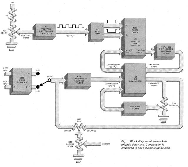
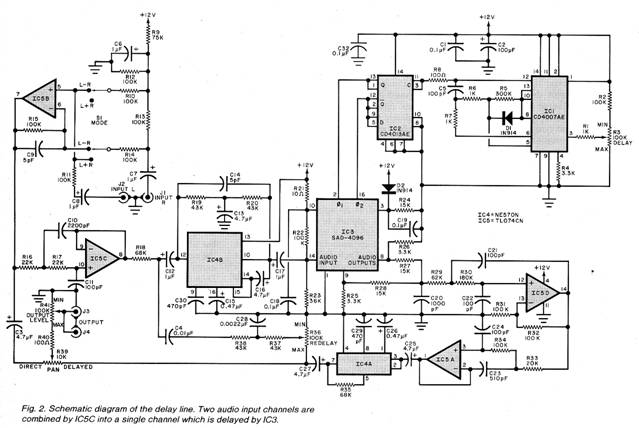
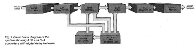
The Analog Audio Delay Line appears in block-diagram form in Fig. I and schematically in Fig. 2. The block diagram shows the principal function stages of the project.
A voltage-controlled oscillator generates a train of pulses at a rate determined by the setting of the DEI\Y potentiometer. The oscillator drives a flip-flop, which provides a two-phase clock signal by means of its complementary (Q and Qj outputs. This two-phase clock governs the transfer of signal samples within the analog shift register.
An op-amp input stage accepts signals from the two main stereo channels and generates either an L+R or L—R output, depending on the position of the MODE switch. A considerable saving in system cost and circuit complexity can be realized by combining the main stereo channels to form one channel of delayed information.
Summing the two main channels before delaying them results in a conventional monaural signal that is then delayed, amplified and reproduced by a single loud speaker. The usefulness of the L — R mode can be dramatically demonstrated by listening to a stereo FM broadcast. During the musical portion of the broadcast, relatively high levels of L + R or stereo reverberation can be introduced to provide a pleasing audio effect. When the announcer’s voice is heard, it sounds as if he is talk ing from the bottom of a well. This can also happen when a centered vocal or instrumental soloist predominates.
The L — R mode, in which the direct center components are cancelled out, can prevent this from happening. An addition al benefit provided by the L — R mode is realized because of the common mix down practice of placing room or ambience microphones and studio reverberation unit output signals away from center. Although it is not possible to completely characterize the differences in sound quality provided by the two modes, the author’s experience is that L — R reverberation sounds “softer” or more subtle. The type of music and the particular mix-down will determine which mode is more pleasing.
The signal from the input network is applied to a second-order active low-pass filter with a cut-off frequency of 15 kHz. This prevents fold back/aliasing problems that might otherwise occur. A 2:1 IC compressor acts on the filter output before it is applied to the analog shift register. Also applied to the compressor input is a signal component that is provided by the recirculation loop.
Delayed audio signals appearing at the output of the analog shift register are treated by a fifth-order active low-pass filter before being processed by a 1:2 IC expander. This filter smooths out the signal provided by the delay line and suppresses any ultrasonic clock energy contained in it. One portion of the expander output makes its way back to the compressor input by means of a recirculation loop. This loop comprises R36, the REDELAY potentiometer, which permits adjustment of the amount of delayed signal fed back to the input compander, as well as a passive bandpass filter (R37, R38, C4 and C28). The bandpass filter provides additional high-frequency rolloff for each recirculation of the signal and some low-frequency rolloff. The accelerated absorption of high frequency components simulates the treble loss of natural reverberation; the low-frequency attenuation prevents the reverberant signal from sounding muddy.
Complementary compression and expansion make it possible for the delay line project to have an impressive dynamic range. The rated S/N of the SAD-4096 analog shift register varies from more than 75 dB for its shortest delays to approximately 65 dB for its longest delay time. The compansion employed in this project allows the delay system to have a very large dynamic range. As measured by the author, the IHF “A” weighted noise at the project’s delayed output is —91.5 dBm at 5 milliseconds and —89 dBm at 100 milli seconds. Input-level adjustments are there fore unnecessary.
Output signals are presented to PAN control R39. This potentiometer allows the user to drive the subsequent stages in the signal chain with a fully undelayed audio signal (when the wiper is set to the DIRECT extreme of its travel), a fully delayed signal (when the wiper is set to the DELAYED extreme of its travel), or with a mixture of the direct and delayed versions of the input signal (when the wiper is set between the two extremes of its travel). Potentiometer R41 can be adjusted for the desired balance of front to back sound levels.
LAST month, we introduced the function and use of audio delay lines— analog and digital—in general. We then described the circuit for a low-cost analog delay line. We continue, now, with the power supply circuits that can be used with that device and construction information.
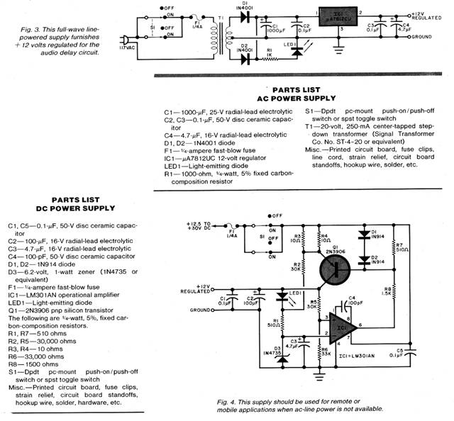
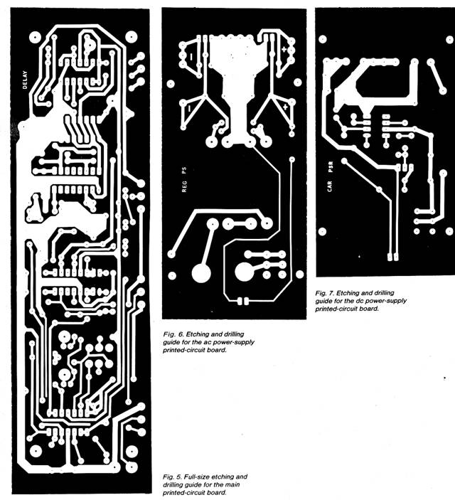
The analog delay line project requires very little electrical power 123 volts (single-ended) at 20 mA. This modest amount of power can be provided by the ac supply shown schematically in Fig. 3. It employs a center-tapped step down transformer, a full-wave rectifier, a few capacitors, and a 12-volt regulator IC. In mobile and many portable applications, however, a source of 117-volt sinusoidal ac is not readily avail able. In such situations, the project can be powered by the dc-powered regulated sup ply shown schematically in Fig~ 4. This supply employs a zener diode as a voltage reference for an LM 301 op amp which in turn governs the operation of a pass transistor. This transistor acts as a regulated source for the delay circuit. The dc supply can be used with an unregulated source delivering from + 12.5 to +30 volts dc.
Construction.
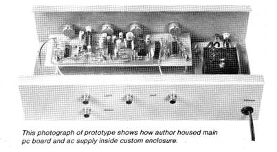
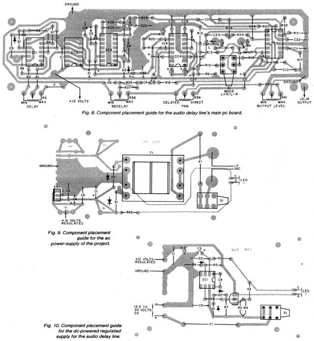
The use of printed-circuit construction techniques is strongly recommended. Full-size etching and drilling guides of suitable pa boards for the main delay circuit, the ac supply, and the dc supply appear in Figs. 5, 6, and 7, respectively. Component placement guides for these boards appear in Figs. 8, 9, and 10. The main circuit board has been laid out to keep power and ground bus runs as short and direct as possible, and to prevent objectionable leakage of ultrasonic clock energy into the audio-frequency signal path.
Sockets or Molex Soldercons should be used when mounting ICs on the main circuit board especially for IC3 any device costing that much deserves special handling. When mounting semiconductors and electrolytic capacitors, be sure to observe polarity and pin basing. Use the minimum amount of heat and solder consistent with the formation of good solder joints. Those components mounted off the board can be connected to it by means of suitable lengths of stranded, insulated hookup wire.
When assembly of the circuit boards is complete, carefully inspect them for cold solder joints, solder bridges between adjacent foils, reversed polarities, etc. Then interconnect the main board with the power supply board that has been assembled, using short lengths of stranded, insulated hookup wire. Finally, mount the boards and other components in a suitable enclosure, with spacers to insulate the boards from the metallic surfaces of the cabinet.
Adding It to Your System.
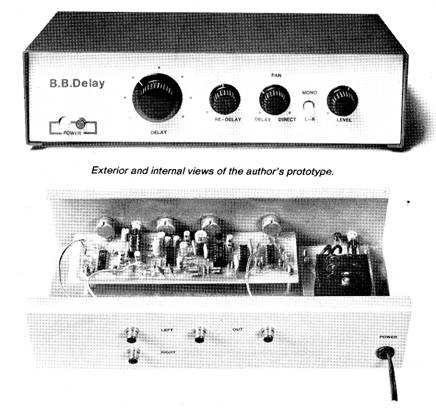
Use shielded audio patch cords of appropriate lengths to interconnect the project with your existing audio system. The main stereo channels should be tapped at some point at which the signals are at line level. If the signals are tapped at the output of the preamplifier, the project’s output level potentiometer can be used as a front-to-back balance control. If the signals are tapped before the preamplifier’s volume control, the project’s output level potentiometer will have to be readjusted every time the level of the front channels is changed.
A single channel of delayed audio information calls for a monophonic power amplifier and one speaker system. However, the author’s prototype includes two output jacks wired in parallel so that both channels of a stereo amplifier can be driven by the same signal if desired. The rear-channel amplifier can have a power rating as low as one fourth of that of the front-channel amplifier. Excellent performance has been obtained with as little as 20 watts of rated amplifier power for the rear channel. Similarly, the speaker system associated with the rear channel need not be as sophisticated as those used in the main (front) stereo channels. Deep bass response and an extended high end are simply not needed. A speaker system with clean midrange response and a power-handling capacity compatible with the rear-channel amplifier output power will suffice.
There are no “correct” delay-unit control settings. These adjustments should be guided by the type of music being reproduced and the personal taste of the listener. Also, the amount of reverberation that will have to be introduced to achieve a desired effect will depend on the individual recording of a given piece of music.
Two discrete delay channels can share a common enclosure and power supply. Such a configuration is available in kit form and can be connected to the main stereo channels in such a way that monaural addition or subtraction will not take place. If desired, one clock can be used to drive both stereo delay lines so that the delay times track each other. A richer sound may result if each channel has an independent, adjustable clock.
In Conclusion.
Psychoacoustics is still as much an art as a science, and remains a fertile field for experimentation. The analog delay line that has been presented here is designed with the adventurous, inquisitive audiophile in mind. It is therefore well suited for those readers who want to experiment with time-delay techniques.
Computer-type RAM memory and both AID and 0/A converters are used in this second approach.
IN the first two parts of this series, we described an audio delay system based on analog techniques using buck et-brigade devices as the principal active elements. This month we will concentrate on the use of digital techniques to achieve the same purpose.
The project described here uses A/D (analog-to-digital) and D/A (digital-to analog) converters, random access memory (RAM), and a time base that provides the necessary synchronization for the digital system as well as deter mining the length of the delay.
Version 2, A Digital Audio Delay Line
Overall Operation. As shown in Fig.1, the audio input is fed to a filter and amplifier combination that attenuates frequencies above 10 kHz (to prevent aliasing problems) and scales the signal level for the A/D converter.
An 8-bit A/D converter performs a companding conversion that increases the digital signal resolution to an equivalent 11 bits plus sign, giving a dynamic range of approximately 70 dB. The converter operates under the control of synchronization pulses from the clock/ controller. Digital information at the output of the A/D converter passes to a 4096 (4K in computer jargon) X 8-bit RAM as a series of 8-bit “words.” Timed by pulses from the clock/controller, the stream of digital words cycles through a desired number of memory locations, up to the maximum of 4096. At any point in the cycle, as an old sample is read from the data latch and passed to the D/A converter, a new sample is written into the memory.
The length of delay is determined by the number of memory locations through which each sample passes and the length of each sampling interval. (The number of locations traversed is set by the manual switches.) For example, if the sampling frequency is 25 kHz, one sampling interval is 1/25,000 second or 40 microseconds. Therefore, if all 4096 memory locations are used, the total de lay will be 4096 X 40 (uS) or 163.84 milliseconds. A 20-kHz rate would give a delay of 204.8 milliseconds.
Setting the memory address counter to some number between 1 and 4096 by means of the thumbwheel switches al lows the delay to be varied while holding the sampling rate constant. Since the sampling rate also determines system bandwidth, changing the delay in this fashion does not affect frequency response. The fact that digital data is not degraded as it passes through the RAM means that the noise and distortion con tent of the output signal is also independent of the delay.
After the user-selected storage period, the digital data is read out of the memory and temporarily stored in a latch circuit that holds the digital data steady for the following D/A converter. Upon receipt of an appropriate timing pulse, the latch passes the digital data to the D/A converter where it is converted back into analog form. This analog signal, now delayed, is filtered to remove any sampling components above 10 kHz that may be present. After filtering, the audio signal is amplified to bring it up to a level (about 1 volt) that can drive an audio amplifier.
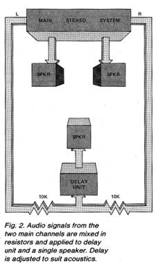
Like the analog unit, the digital delay system is intended to be used with one or two auxiliary power amplifiers and loud speakers. Ideally, there should be two delay units, one per channel. The signal should be delivered to your listening area at a level about 10 dB below that of the undelayed sound. For reasons de tailed in Part 2, less expensive speakers and amplifiers can be used for the delayed sound channels.
To further economize, a single amplifier, speaker, and delay unit can be used. Audio from the two main channels can be resistively mixed and fed to a single delay unit as shown in Fig. 2.
The length of the delay produced by the unit can be adjusted in small increments to tailor it to the acoustics of your listening area. Start with about 20 milliseconds and experiment from there. Pro vision has been made to feed some of the output signal back to the input to generate reverberation. But if there is too much feedback, oscillation will occur.
Circuit Description.
Due to its complexity, the circuit has been broken up into small, functional units. The individual circuits are interconnected by mating “letters-in-a-circle.”
Input Filter and AID Conversion. As shown in Fig. 3, IC1a and ICIB form a low-pass filter that amplifies all signals below 10 kHz. A comparator formed by ICI C monitors the amplified signal and turns on LED1 when the audio reaches the optimum four volts peak-to-peak.
The amplified signal from IC1b (pin 7) is passed to an A/D converter consisting of IC2A, IC18 IC22 IC24 and two of the gates in IC23 Timed by a “start conversion” pulse from the clock/controller, the incoming analog audio is converted into 8-bit binary code that is presented to the RAM for temporary storage. The converter performs a cornpanding action, making the resolution of the digital signal equivalent to an 11-bit word plus sign. Dynamic range is thus approximately 70 dB.
Memory and Latch. This circuit, shown in Fig. 4, uses eight conventional 4096 (bits) by 1 (bit) static RAMs (IC3 through IC10 arranged to form a 4096 (bits) X 8 (bits) array. Static RAM is used to avoid the refresh cycles needed by dynamic RAM.
Each RAM element has its own unique address identified by the “An” (n stands for a digit) symbol above each RAM address line pin. Each RAM also has one pin (pin 8, R/W) that enables the RAM to accept data when the signal on this pin is in one logic state, and out put the data when the pin is in the opposite logic state. Thus, under control of pulses from the clock/controller, the RAM can read in external data, or write out the data contained within its cells. The eight bits of data passed out of the RAM go to a pair of four-input data latches IC11 and \I that hold the data in their internal flip-flops until a properly timed pulse from the clock/controller causes it to pass to the D/A converter.
D/A Converter and Output Stages. The data from the RAM/latch circuit is applied to IC13 a D/A converter, as shown in Fig. 5. The reconstructed out put signal from the D/A converter is almost identical to the filtered analog input, except that it is multiplied by a small scaling factor (due to amplification), contains a small amount of “quantization” noise caused by the D/A con version, and, of course, is delayed.
After amplification in IC25a brings the signal up to about 1-volt peak-to-peak, the analog signal is passed through an active low-pass filter com posed of IC25b and IC25c. The filter cuts off at 10 kHz, and attenuates any sampling frequency components that may remain in the signal. The output of IC25c is then used to drive the external audio amplifier.
Clock and Controller.
The system clock, implemented by ICI 9 in Fig. 6, is the basic timing control for the system. Its main element is a vco (voltage-controlled oscillator) whose frequency is determined by the setting of R21 Varying the clock rate allows the user to experiment with effects such as vibrato, flanging, or frequency modulation. Keep in mind that the vco not only affects delay time but system bandwidth as well.
Counter IC17 accepts the clock signal and is configured to generate the four timed trigger pulses used by the. A/D converter, RAM memory, and data latch. The four outputs are buffered by elements of IC20 and IC21 to convert the low-current CMOS outputs of IC17 7 into signals capable of driving TTL.
As shown in Fig. 6, the four timing pulses are identified as P1, P2, P3, and P4. Pulse P1 commands the start of an A/D conversion in ICl8 (Fig. 3), while P2 increments (by 1) the memory ad dress counter of Fig. 7. The resulting memory address points to the oldest stored sample. A new conversion will be completed eight clock pulses after P1.
The RAM is normally in the read mode, which means that the memory constantly displays the 8-bit code stored at the address pointed to by the memory address counter at its output. The third pulse, P3, is applied to the data latches (Fig. 4), causing them to load the result of the read operation and hold it stable for D/A conversion by IC13 (Fig. 5), which takes place in less than one micro second. The last pulse, P4, causes a memory write operation that overwrites the old sample with the 8-bit code currently available at the A/D converter output.
Delay Switching. The delay switching uses three ICs to select the RAM memory addresses dialed in via the user-accessible switches as shown in Fig. 7.
Programmable counters IC14, IC15, and IC16 are cascaded with the clock input presented to IC16 Its “carry” out put drives IC15, which in turn drives IC14, These counters can be preset to any desired modulo output by entering the control data on the input pins—in this case, voltage or ground from the user-selectable switches connected to S2 and S3. Thus, the outputs of each IC will agree with the manually preset count, independent of the clock frequency. Since there are 12 address lines, the count can reach a maximum of 211 + 210 +2g. . .+2°=2’2—1=4095and the delayed bits can pass through any desired number of memory locations.
Power Supply. The power supply, shown in Fig. 8, uses a full-wave rectifier in conjunction with —12, +12, and + 5-volt regulators. The system draws 450 mA at + 5 volts, and about 20 mA from each of the 12-volt supplies.
The 5-volt power requirement can be reduced by using “LS” or “C” versions of IC11 IC12 IC14, IC15 and IC16. Do not use “L” devices because these usually have different pinouts. Regulators IC27 and IC28 should be supplied with heat sinks.
Construction.
Given the complexity of the circuit, construction is best implemented by using either Wire-Wrap Techniques or a printed circuit board. In the former case, care should be exercised concerning the ground connections. As shown in the schematics, the analog digital grounds should be isolated from each other and merge only at the power supply common point.
Due to their size, etching and drilling guides and component layout for a double-sided pc board for the project are not reproduced here, but can be obtained by sending a self-addressed 9-by-12 envelope with two units of first-class postage to Dept. DDL, Editorial, POPULAR ELECTRONICS, One Park Ave., New York, NY 10016.
Outputs of the address counters (IC14, IC15, and IC16) should be kept as short as possible and as far away as possible from the input and output op amps. The use of IC sockets is recommended, and the proper installation of polarized elements must be observed.
After the board is completed, it can be installed in a suitable metal enclosure and interconnected as shown in Fig. 9. Although this illustrations shows a pair of thumbwheel switches used to select the delay, DIP switches, such as those used in computer boards, can be substituted. The input gain control, R43, output gain control, R44, reverberation control, R45, audio connectors, J1 and J2, peak indicator, LEDI, and the two delay-select switches can be mounted on the front panel. For stereo, dual potentiometers are used for R43 through R45, along with two sets of thumbwheel switches and two peak indicator LEDs.
Adjustment.
With the delay unit connected to an audio system as shown in Fig. 2, set R14 and R21 to their center positions. Place the delay switches (S2 and S3) in the minimum configuration (all switches open). Then adjust echo (reverb) potentiometer R45 for its mini mum resistance, and the audio input control (R43) to its center rotation position.
Increase the audio input level, either by adjusting R43 or the audio signal generator’s level control, until some clipping is noted on the output waveform. Successively adjust the input level and R14 to obtain a symmetrically clipped sine wave. Then reduce the input level to just below clipping, so that a clean sine wave is displayed.
Increase the sine-wave input frequency to 5 kHz and adjust R21 to minimize any serrated edges on the displayed waveform. Besides reducing noise, this adjustment also controls the sampling frequency (and bandwidth).
If an oscilloscope is not available, you can perform these adjustments by ear. Preset switches S2 and S3 for the desired amount of delay. Use a source of actual program material in place of the signal generator and your ears as “distortion monitors.” Adjust the potentiometers for best audible performance. The results obtained by this method will, of course, be less accurate, but will be useful if care is taken in performing the adjustments.
With proper audio input levels, a 4 volt peak-to-peak signal should be seen at pin 7 of ICIB (A/D converter input). If you should require more gain, the value of R1 (feedback resistor for IC1a) can be increased.
The memory address counter (IC14, IC15, IC16) can be checked by setting S2 and S3 for maximum delay. This causes each of these IC’s to count down by 16. An oscilloscope or frequency counter can then be connected to the A0 through All outputs of these ICs to note the decreasing frequencies.
A scone can also be used to follow the audio signal through to the A/D converter. The digital outputs of IC18 vary with the applied audio signal. If a dc voltage level from zero to about 1 volt is applied to the input, the bit changes can be observed as the input voltage level is changed. Zero volts will produce all zeroes and 1 volt will create all ones, with 254 binary states between the two.
|


 Apply
a 1-kHz sine-wave signal to the audio input (J1), and an
oscilloscope to the J2 audio output connector. With power turned on,
adjust output control R44 for a convenient scope display.
Apply
a 1-kHz sine-wave signal to the audio input (J1), and an
oscilloscope to the J2 audio output connector. With power turned on,
adjust output control R44 for a convenient scope display.Copyright by Bill Bytheway, K7TTY February 2012