|
DIGITAL IC TESTER
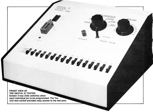
This unit tells you if the trouble is in the IC or in your circuit design
JOHN W. RASMUSSEN
IF YOU ARE INVOLVED WITH DESIGNING AND OR building digital circuit projects, you have undoubtedly, at one time or another, encountered a situation in which the project doesn’t work and in which you are left with the task of deciding if it is one of the IC’s that doesn’t work or if it is a faulty design that is the cause of the failure of the project.
In such situations it would be handy to have a permanent setup, where you can test all kinds of digital IC's without having to spend a lot of time on wiring, etc. Such a setup would also be helpful in checking out IC's bought surplus, but of unknown quality.
The article presented here, describes the construction of a manual digital IC tester, that will fill this need. With this tester you will be able to check the operation of any 14- or 16-pin digital IC with ease and speed. Both CMOS and TTL circuits can be tested with this unit.
The basic principle of the tester is to have an array of 16 slide switches that allow each individual pin on the IC to be tested. The switches connect each pin to either GND, CLOCK or may be left open. The pins of the test socket are also connected to the corresponding pins on another 16-pin IC socket. This one serves as an output socket. It makes it possible for the user to connect components to the IC under test. This makes it possible to test astable and nonostable multivibrators in operation. It also allows external feedback paths in testing of counters and applying loads to drivers, LED drivers, etc.
Circuit description
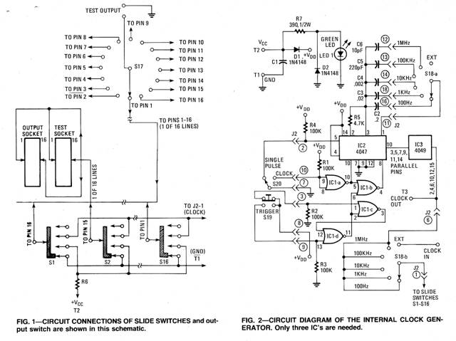
Figure 1 shows how the slide switches are connected to the test socket, as described in the introduction. Switch S17 is a rotary switch that connects the test output terminals to any one of the 16-pins on the test socket. The output test terminals can be connected to a scope, a DVM or other test instrument to check out the operation of the IC under test.
Although only 16 positions are needed on Sl7. a 23 position switch is used because it allows a smaller angle of rotation, which makes the front panel legend easier to read. Adjustable stops on the switch limit the rotation to 16 positions.
Figure 2 shows the circuit diagram of the internal clock generator. IC2, a 4047, forms the basic oscillator circuit. Its mode of operation is controlled by S20. When S20 is in SINGLE PULSE, pin 5 of IC2 is grounded. This makes IC2 operate in the monostable mode. In this mode IC2 is triggered on the rising edge of a positive pulse on pin 8. Two sections of IC1 form a de bouncing circuit for S19 which acts as a manual trigger for IC2.
When S20 is in CLOCK. IC2 operates in the astable mode. In this mode pin 10 of IC2 is held high. This, in turn, inhibits the operation of the trigger input. The clock frequency is controlled by R5 and C2 through C6 and covers the range of 100 Hz to 1 Mhz. At the 1-Mhz setting, however, the operating frequency will to a substantial degree be dependent on operating voltage VCC. At VCC = 5V the operating frequency will be only about 600 Khz, rising to 1 MHz when VCC = 10V. This is due to limitations in the 4047.
IC 3 acts as a buffer, using six paralleled sections of the 4049, yielding a fan-out of 12 TTL loads. Diode D1 protects the clock generator against damage in case of polarity reversal of C1 is a filter capacitor. LED1 is a green LED indicator. It shows correct polarity of VCC. Diode D2 protects LED1 against reverse break down damage. It may or may not be required, depending on the specifications of the LED that you use. One section of Sl8 switches capacitors C2 through C6. The other section of S18 selects the internal or external clock for clocking the IC under test.
Assembling your tester
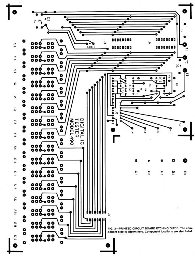
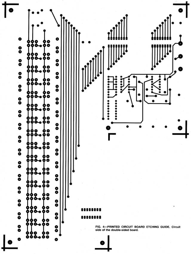
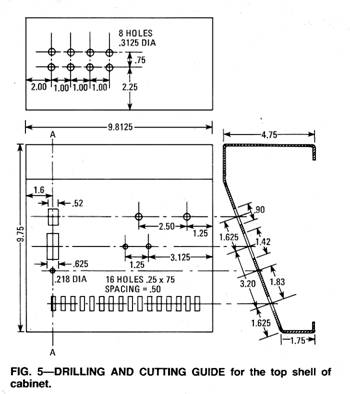
The first thing to do is to get all the parts together. You’ll find a complete parts list and a list of suppliers in this article. The circuit board you may etch yourself using the layouts in Fig. 3 and Fig. 4. A guide to drilling and cutting the cabinet is in Fig. 5. The printing on the cabinet may be done using dry transfer letters. available in most artist-supply stores. The lines are done with thin adhesive drafting tape.
Before lettering the cabinet, drill and cut all of the holes. Then spray the top shell of the cabinet with an antique white flat enamel.
The original paint of the cabinet is semigloss, which is not very receptive to the dry transfer lettering. By spraying first with a flat enamel, any problem with the lettering is virtually eliminated.
After the lettering, spray the top shell of the cabinet with two or more coats of a clear matte finish. These coats should be thin to prevent any possible loosening of the lettering.
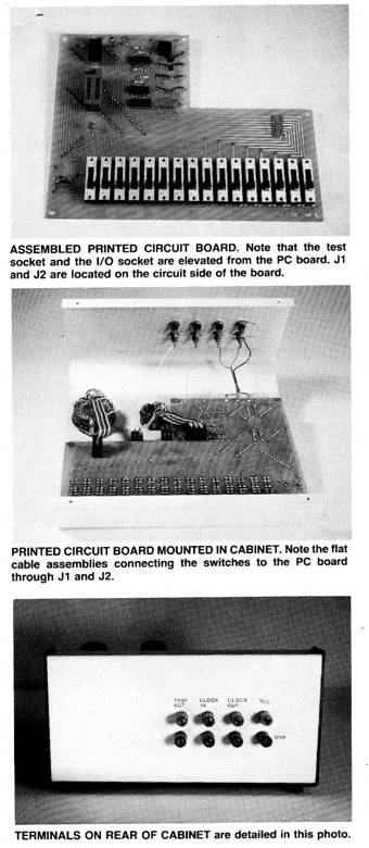
The assembled PC board can be seen in the photos. If you etch your own PC board, all of the pads around the feed-through holes will have to be connected by a wire. This is simple. Just take four holes at a time and put a short 22-gage wire through the holes. Then bend the wires on one side of the board, lay the board flat against a table and solder the top pads. Next, turn the board over and solder the bottom pads. Continue until all the feed-through holes are soldered.
Under the slide switches is a feed-through hole. It was located there to avoid having to solder the top pads on these switches. These pads are inaccessible after the switches are mounted on the PC board, so if you etch your own PC board, the feed-through holes under the switches must be soldered before mounting the switches. J1 and J2 are 16-pin IC sockets mounted on the reverse side of the PC board and provide connections to the rotary switches. Note in the internal view the flat cable assemblies, connecting the switches to the PC boards through J1 and J2.
All of the GND terminals on the rear of the cabinet are tied together and then tied to the cabinet and the TI terminal on the PC board.
To avoid screw holes in the front panel, the PC board is mounted on stand-offs bonded to the inside of the cabinet with clear Silicone Rubber sealant.
A portion of the sealant is then placed at the markings of the spacers after first removing the PC board with the spacers. After the sealant has been deposited, the PC board with spacers is again positioned inside the cabinet and temporarily held in place by tape. The sealant is worked in around the body of the spacers to provide maximum support and adhesive. After allowing 12 hours for drying, the tape may be removed.
The test socket and the I/O socket is elevated from the PC board. These sockets are soldered to the PC board after being positioned correctly, with the PC board mounted inside the cabinet.
Put the tester to work
The majority of IC's - gates, counters, decoders and multiplexers—do not require any external components for performance testing. One-shots, line drivers and 7segment LED drivers do require external components for testing. The I/O socket makes this possible. It gives direct access to all of the pins of the IC.
As an example, if you want to check out a one-shot, you may use a DIP plug-in module to hold the timing components for the one-shot. The trigger can be either CLOCK or a SINGLE PULSE.
Another example would be the check-out of a
7-segment LED driver. In such a case you would need a 7segment LED,
some resistors and possibly a counter to drive the 7-segment LED
driver. These components could be mounted on
The clock for driving the counter may be taken from the CLOCK OUT terminals on the back of the cabinet. A test sheet could be made, listing the pin connections for various IC's That would eliminate the need for reference to the data sheets and speed up the testing.
As you can see, this versatile tester will allow you to check out the operation of a wide variety of IC's with minimum efforts.
|
 First
six 0.5-inch hex spacers are mounted to the PC board with screws.
The assembled PC board with the spacers mounted are then held in
place with tape. while the positions of the spacers are marked with
pencil on the inside of the cabinet.
First
six 0.5-inch hex spacers are mounted to the PC board with screws.
The assembled PC board with the spacers mounted are then held in
place with tape. while the positions of the spacers are marked with
pencil on the inside of the cabinet.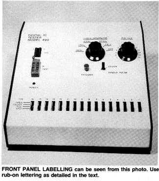 a solderless breadboard and connected to my Digital IC Tester by a
DIP cable.
a solderless breadboard and connected to my Digital IC Tester by a
DIP cable.Copyright by Bill Bytheway, K7TTY February 2012